


In this article, describe analyzing theoretically temperature and dopimg dependence built in voltage in silicon solar cells.
Key words: Built-in voltage, semiconductors, solar cell, temperature, doping concentration
The size of the internal potential is one of the important parameters for all solar cells. The function of the internal potential is to move electrons and holes from one field to another. Of course there is talk of the existence of two such forces in the motion propositions of electrons and holes. But the most important of these is the internal potential of the impoverished zone. We know that the first field gives the first-order integral potential along the coordinate axes. The question is, how is the internal potential created? Does ordinary silicon also have internal potential? No ordinary silicon element has no internal potential. The internal potential is also called the potential barrier by another name. The potential barrier separates the electrons and holes generated by the light in the solar cells and creates a voltage. There are different ways to create a potential barrier in solar elements. The most popular of these is the p-n junction.
The potentials of charged particles in the medium are determined by the Poisson equation [1].
 (1)
(1)
Here:
ρ — charge density
φ — potential
ε — dielectric permittivity
 (2)
(2)
We can determine the internal potential either by the pits or the concentration of electrons. That is, we can determine the concentration of holes in area p by the ratio of the concentration of holes in area n.
![]() (3)
(3)
The concentration of holes in the P area is approximately equal to the acceptor concentration in this area.
 (4)
(4)
The concentration of pits in area N is equal to the ratio of the square of the concentration of specific charge carriers to the donor concentration.
![]() (5)
(5)
The concentration of electrons in the N field is approximately equal to the concentration of the donor input in this field.
 (6)
(6)
The concentration of electrons in the P field is equal to the ratio of the square of the specific charge carrier concentration to the acceptor input concentration.
 (7)
(7)
Given the above expressions, the potential barrier value is a magnitude dependent on the input concentration and temperature. However, it can be seen from Equation 7 that the potential barrier is linearly related to temperature, but this is not the case. This is because the concentration of specific charge carriers is strongly related to temperature [3].
 (8)
(8)
Here:
T — temperature
Eg — band gap
k — Boltsman constant
This means that as the temperature increases, the concentration of specific charge carriers also increases sharply.
If we say that the potential barrier is formed at the p-n junction, then the charge carrier concentration, potential, and internal field strengths are distributed as follows.
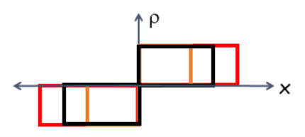
Fig. 1. Coordinate dependence of the concentration of charge carriers in the P-n junction
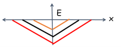
Fig. 2. Coordinate dependence of the internal field strength at the P-n junction
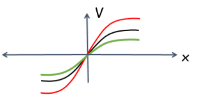
Fig. 3. Coordinate dependence of the internal potential at the P-n junction
All of the above diagrams are for the impoverished zone at the p-n junction. From this we can conclude that the potential value at the center of the impoverished zone of the p-n junction is zero. That is why this line is called the transition line. The concentration of the charge carriers changes along the transition line. The modulus of field strength reaches its maximum value at the transition line. This allows the generated electrons and holes to separate.
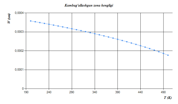
Fig. 4. Temperature dependence of the width of the impoverished zone
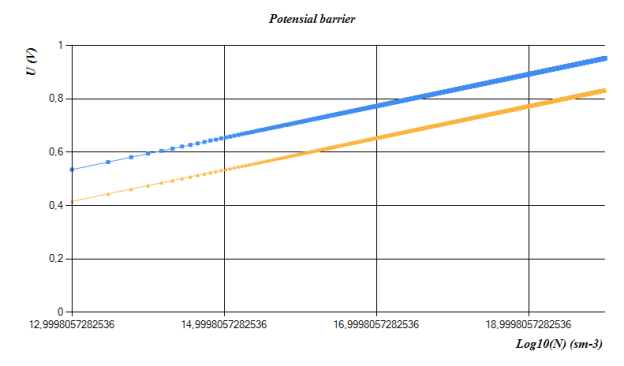
Fig. 5. Dependence of potential barrier on input concentration
Today, computing technology is developing rapidly. Digital technologies are widely used in every field. The advantages of this are less time spent on calculations and increased calculation accuracy. Theories never come into being by themselves. They are also based on the results obtained in the experiment [2]. I think that if we can organize the chain of theories correctly, we can get information about a lot of the properties of the object we are studying. I created a chain of such theories and created a program called Suntulip-2 for silicon solar cell. The program is easy to use and can be used by people who have no knowledge of programming. Using this program, we determined the reduced zone width as well as the potential barrier of a solar cell with the following parameters.
NA = 1e15
ND = 1e17
dn = 100 nm
dp = 200 mkm
In conclusion, the magnitude of the potential barrier in solar cells is strongly related to the input concentration.
References:
- A. Luque, and S. Hegedus, Handbook of photovoltaic science and engineering, p. 148: John Wiley & Sons.
- J. C. C. Fan, “Theoretical temperature dependence of solar cell parameters,” Solar Cells, vol. 17, no. 2–3, pp. 309–315, 1986.
- S. Sze, Physics of semiconductor devices, 3rd ed., p. 109: John Wiley & Sons, Inc., 2006.
