


In this paper, the simulation of field enhancement near the tapered gold tip as an optical antenna and quantum efficiency of Cadmium selenide (CdSe) quantum dot, which is located in the near field of gold tip antenna, are presented. We show the possibility of change of quantum efficiency of quantum dot, also optimized geometry of our antenna for obtaining the maximum of quantum efficiency.
Keywords: quantum efficiency, optical antenna, cdse quantum dot, tapered gold tip, electric field enhancement
1. Introduction
Many studies have considered the luminescence of colloidal II–VI nanocrystals, the photoluminescence (PL) and electroluminescence emission from colloidal cadmium selenide (CdSe) quantum dots (QDs) by controlling nanocrystal size can be tuned within the visible spectrum from wavelengths of 450 nm to 650 nm. This versatility opens up a variety of potential applications for CdSe quantum dots in photonic devices, such as emitters for color displays, color modifiers for light emitting diodes (LEDs) [1], optical fiber amplifiers [2], low threshold lasers [3], self-assembled photonic sphere arrays [4], polymer-based photovoltaic cells [5], optical temperature probes [6], chemical sensors [7] and high-speed signal-processing filters [8]. Under optical excitation, quantum dots’ capacity for bright emission is quantified by the photoluminescence quantum yield, defined as the ratio of emitted photons to absorbed photons. Thanks to the progress in wet chemistry, highly luminescent semiconductor nanocrystals have been achieved [9, 10]. One of their most interesting properties lies in the three dimensional carrier confinement effects [11]. By varying their size, the emission wavelength can be tuned in the visible and the near-infrared spectrum. An important practical figure of merit in the context of nanocrystal synthesis optimization is their fluorescence quantum efficiency [12–14]. The quantum efficiency of a fluorophore is defined as the ratio of the number of emitted photons divided by the number of absorbed photons. Demas and Crosby [15], reviewed quantum yield measurement methods in solution in 1970.Quantum efficiency of cdse is low One way to increase the quantum efficiency dots is a conception of optical antenna [16]. An effective antenna interacts strongly with incoming radiation and leads to a high degree of field localization. The localized fields have been used in several recent experiments as an excitation source for local spectroscopy such as fluorescence, IR-absorption and Raman scattering. The antenna typically lead to an increase in excitation rate due to local field enhancements and the associated increase of the local density of states. There for antenna-induced increase in fluorescence is a result of an increase in the Excitation rate [17]. In this paper, we used the method FDTD for simulation of the quantum efficiency of cdse nanocrystal by using of lumerical software. We discuss the simulation method and configurations of chosing geometry. We designed special optical antenna, i.e. a Gold tip with a radius of 10nm and the angle of cone 30 deg and the circular grating with periodicity of 200nm on the shaft of the tip. The quantum efficiency of a cdse quantum dot with 5 nm diameter is simulated in different situations. The quantum efficiency of cdse nanocrystals, by considering of nanocrystal and optical antenna in a vacuum, is then theoretically obtained.
2. Resultand discussion
Finite-difference time-domain approach is a reliable method for solving Maxwell’s equations in complex geometries [18]. FDTD provides time domain information, offering insight into electrodynamics of the system [19]. In FDTD, the electromagnetic field and structural materials of interest are described on a discrete mesh composed of so-called Yee cells. Maxwell’s equations are solved discretely in time, where the time step used is related to the mesh size through the stability criterion. This technique is an exact representation of Maxwell’s equations in the limit that the mesh spacing goes to zero. The calculated and reported intensities are normalized with respect to the intensity of the incident light. In side illumination, the light is linearly polarized along the tip axis. The software “LUMERICAL” based on FDTD theory was used.
Field enhancement near Nano scale metal structures plays a major role in optical phenomena the enhancement originates from the combination of the electrostatic lightning-rod effect, due to the geometric singularity of sharply pointed structures, and localized surface Plasmon resonances [20]. The incident light drives the free electrons in the metal along the direction of polarization. Enhanced field is confined to the apex-tip in all three dimensions. Thus, the illuminated tip represents a nanoscale light source. To generate a strong field enhancement at the tip, the electric field of the exciting laser beam needs to be polarized along the tip axis. The influence of tip shape and material on the field enhancement has been discussed in a series of publications with the aim to find the optimum tip [21]. The number of excitations relaxed radiatively from excited states to the ground state determines the PL intensity. The enhancement of PL therefore depends on the excitation rate and the Quantum yields Q denoting the fraction of emitted photons Accordingly, the PL enhancement due to the presence of the metal tip can be written as [22]. During a near field measurement, both radiative decay rate and non-radiative decay rate are affected by the presence of the metal structure: radiative decay is modified in the enhanced field at the Molecule location (Purcell effect) [22–23] and non-radiative is increased by non-radiative decay channels Created by energy dissipation inside the metal tip [22, 24]. This QPL can be significantly increased. The presence of the tip as the enhanced rate radiative decay rate will predominantly increase the quantum yield. Such enhancement is not possible for systems with a quantum yield already close to 1, such as Fluorescent dyes, or quantum dots.
Since the distance between the emitter and metal tip is very small, non-radiative Transfer of energy from the electronically excited molecule to the metal followed by non-radiative Dissipation has to be taken into account. This process represents an additional non-radiative Relaxation pathway and can extinguish the fluorescence. While the theory of energy transfer Between molecules and at metal interfaces is well understood in the framework of phenomena logical Classical theory [24, 25], nanometer sized objects are more difficult to describe. Tip-induced radiative rate enhancement and quenching has been studied in literature theoretically [26, 28]. Experiments on model systems formed by single molecules and spherical metal Particles revealed a complex distance dependent interplay between competing enhanced and Quenching processes [29, 30]. Small cone angles in tip-shaped metal structures are expected. To reduce energy dissipation as compared to spherical particles [28], in the ordinary TENOM direct illumination of apex,results in generation of background signal and increasing of noise. Different approach is used for decreasing of this background signal, such as adiabatic nanofocusing [31]. Adiabatic nanofocusing along conical metal tapers describes a coherent transport of optical excitations in the form of surface plasmon polariton (SPP) waves over several tens of  m and the concentration of this energy into a nanometric volume at the taper apex [32,33]. From an application point of view, adiabatic nanofocusing results in the creation of a single, dipole-like emitter, spatially localized to a few nm and with an intense optical near field. Such an emitter holds a high potential for, e.g., ultrahigh resolution optical microscopy, tip-enhanced Raman spectroscopy, or extreme ultraviolet (EUV) generation.
Sharp conical gold tapers are of particular importance for providing nanometer-sized light sources for scattering-type scanning near field optical microscopy (s-SNOM) [34–36]. Generally, nanoslit gratings, milled onto the taper shaft at distances of up to several tens of microns from the taper apex, are used to couple far field light onto the taper and to launch SPP waves. This distance is a compromise between achieving a virtual background-free nanolocalized light source at the apex and minimizing SPP propagation losses. With such tapers, it could so far be shown that the spatial extent of the nanofocused light source can be reduced to less than 10 nm in the figure 1 our antenna is shown. In the next, grating of antenna is illuminated with a plane wave laser and enhancement of the intensity near the apex is simulated for two periods of grating. In the figure 2, enhancement of intensity is shown in period (a) 200 nm and (b) 300 nm. Localization of energy occurs in the region with dimension approximately 10 nm around the apex. Then we insert a cdse quantum dot with 5nm diameter in the near field of the antenna. Distance of center of quantum dot from apex is considered 10 nm and quantum efficiency of its simulated in two situations. In figure 3 the result of its simulation is shown. As we see, with change of geometry of the antenna, quantum efficiency is varied. Now, we want to optimize antenna and obtain the maximum of efficiency. If we do not change parameters such distance of quantum dot to apex and only vary grating, we can know optimized period of grating and get maximum of efficiency. In figure 4, results of optimization are shown. In a we have, maximum of enhancement of intensity and as we result,quantum efficiency for this amount will be maximum as shown in the b.
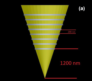
Fig.1. Design of optical antenna
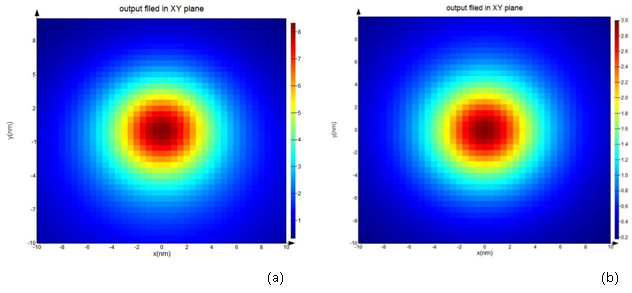
Fig.2, Enhancement of electric field in plane x-y for antenna with a) 200nm and b) 300 nm period of grating
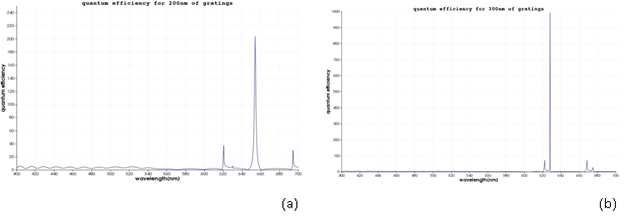
Fig.3, quantum efficiency for (a) period 200 nm and (b) 300nm
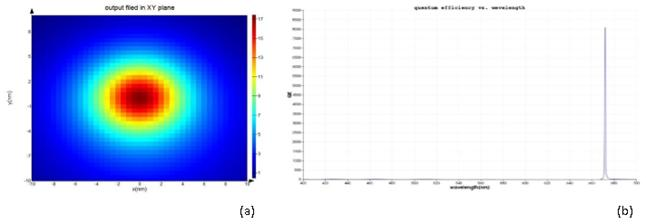
Fig.4, (a) Enhancement of electric field in plane x-y for antenna with 208.380nm period of grating(optimized),(b) quantum efficiency for this amount
3. Conclusion
Using FDTD simulation, enhancement of the electric field near gold tip in different conditions and the change of quantum efficiency of a quantum dot under the just apex of gold tip obtained in two configurations of tip. Maximum of quantum efficiency in this form of optical antenna correspond to period of granting equal to 208 nm.
References:
1. Hasegawa, Yasuo. «Light diffusion type light emitting diode». U. S. Patent No. 5,140,220. 18 Aug. 1992.
2. Inagaki, Shinya, et al. «Optical fiber amplifier». U. S. Patent No. 5,136,420. 4 Aug. 1992.
3. Marko Loncˇar, Tomoyuki Yoshie, and Axel Scherer, «Low-threshold photonic crystal laser». Applied Physics Letters 81.15 (2002): 2680–2682.
4. E W Seeliga, B Tanga, A Yamilovb, H Caob, R. P. H. Chang, «Self-assembled 3D photonic crystals from ZnO colloidal spheres». Materials Chemistry and Physics 80.1 (2003): 257–263.
5. Coakley, Kevin M., and Michael D. McGehee. «Conjugated polymer photovoltaic cells». Chemistry of materials 16.23 (2004): 4533–4542.
6. C Durney, C Johnson, J Lords, TC Rozzell, «Optical temperature probe». U. S. Patent No. 4,016,761. 12 Apr. 1977.
7. Lončar, Marko, Axel Scherer, and Yueming Qiu. «Photonic crystal laser sources for chemical detection». Applied Physics Letters 82.26 (2003): 4648–4650.
8. M Sugawara, T Akiyama, N Hatori, Y Nakata, H Ebe and H Ishikawa. «Quantum-dot semiconductor optical amplifiers for high-bit-rate signal processing up to 160 Gb s-1 and a new scheme of 3R regenerators».Measurement Science and Technology 13.11 (2002): 1683.
9. Murray, C.B.; Norris, D.J.; Bawendi, M. G. Synthesis and characterization of nearly monodisperse CdE (E = S, Se, Te) semiconductor nanocrystallites. J. Am. Chem. Soc. 1993, 115, 8706–8715.
10. Rosenthal, S.J.; McBridea, J.; Pennycook, S.J.; Feldman, L. C. Synthesis, surface studies, Composition and structural characterization of CdSe, core/shell and biologically active nanocrystals. Surf. SCI. Rep. 2007, 62, 111–157.
11. Price, Peter J., and Frank Stern. «Carrier confinement effects». Surface Science132.1 (1983): 577–593.
12. Qu, L.; Peng, X. Control of photoluminescence properties of CdSe nanocrystals in growth. J. Am.Chem. Soc. 2002, 124, 2049–2055.
13. Deka, S.; Quarta, A.; Lupo, M.G.; Falqui, A.; Boninelli, S.; Giannini, C.; Morello, G.; de Giorgi, M.; Lanzani, G.; Spinella, C.; Cingolani, R.; Pellegrino, T.; Manna, L. CdSe/CdS/ZnS
14. Double shell nanorods with high photoluminescence efficiency and their exploitation as bio-labeling probes. J. Am. Chem. Soc. 2009, 131, 2948–2958.
15. Donega, C.M.; Hickey, S.G.; Wuister, S.F.; Vanmaekelbergh, D.; Meijerink, A. Single-step synthesis to control the photoluminescence quantum yield and size dispersion of CdSe anocrystals. J. Phys. Chem. B 2003, 107, 489–496.
16. Demas, J.N.; Crosby, G. A. The measurement of photoluminescence quantum yields. A review.J. Phys. Chem. 1971, 75, 991–1024.
17. Palash Bharadwaj, Bradley Deutsch, and Lukas Novotny.Optical Antenna 2009 Optical Society of America
18. A. Taflove and S. C. Hagness, in Computational Electrodynamics: the Finite — Difference Time — Domain Method (Artech House, 2000).
19. B. C. Galarreta, I. Rupar, A. Young, and F. Lagugné-Labarthet, “Mapping hot-spots in hexagonal arrays of metallic nanotriangles with azobenzene polymer thin films,” J. Phys. Chem. C 115(31), 15318–15323 (2011).
20. Willets, Katherine A., and Richard P. Van Duyne. «Localized surface Plasmon resonance spectroscopy and sensing». Annu. Rev. Phys. Chem. 58 (2007): 267–297.
21. Gerton JM, Wade LA, Lessard GA, Ma Z, Quake SR. Phys Rev Lett. «Tip-enhanced fluorescence microscopy at 10 nanometer resolution». Physical review letters 93.18 (2004)
22. A. Hartschuh, M. R. Beversluis, A. Bouhelier, and L Novotny. Tip-enhanced optical spectroscopy. Phil. Trans. R. Soc. Lond. A, 362:807–819, 2004.
23. S. K¨uhn, U. Hakanson, L. Rogobete, and V. Sandoghdar. Enhancement of single molecule fluorescence using a gold nanoparticle as an optical nano-antenna. Phys. Rev. Lett., 97:017402–017405, 2006.
24. R. R. Chance, A. Prock, and R. Silbey. Lifetime of an emitting molecule near a partially reflecting surface. J. Chem. Phys., 60:2744–2748, 1974.
25. W. L. Barnes. Fluorescence near interfaces: the role of photonic mode density. J. Mod. Opt., 45:661–699, 1998.
26. N. A. Issa and R. Guckenberger. Fluorescence near metal tips: The roles of energy transfer and surface plasmon polaritons. Optics Express,, 15:12131–12144, 2007.
27. M. Thomas, R. Carminati, J. R. Arias-Gonzalez, and J.-J. Gre_et. Single-molecule spontaneous emission close to absorbing nanostructures. Appl. Phys. Lett., 85:3863{3865, 2004.
28. L. Rogobete, F. Kaminski, M. Agio, and V. Sandoghdar. «Design of plasmonic nanoantennae for enhancing spontaneous emission». Optics letters 32.12 (2007): 1623–1625.
29. P. Anger, P. Bharadwaj, and L. Novotny. Enhancement and quenching of single molecule uorescence. Phys. Rev. Lett., 96:113002{113006, 2006.
30. P. Bharadwaj, P. Anger, and L. Novotny. Nanoplasmonic enhancement of single molecule uorescence. Nanotechnology, 18:044017{044022, 2007.
31. S Berweger, J M. Atkin, R L. Olmon, and M B. Raschke. «Adiabatic tip-plasmon focusing for nano-Raman spectroscopy». The Journal of Physical Chemistry Letters 1.24 (2010): 3427–3432.
32. D. K. Gramotnev and S. I. Bozhevolnyi, «Plasmonics beyond the diffraction limit», Nature Photonics 4, 83–91 (2010).
33. A. J. Babadjanyan, N. L. Margaryan, and K. V. Nerkararyan, «Superfocusing of surface polaritons in the conical structure», Journal of Applied Physics 87, 3785–3788 (2000).
34. C. Ropers, C. C. Neacsu, T. Elsaesser, M. Albrecht, M. B. Raschke, and C. Lienau, «Grating-coupling of surface plasmons onto metallic tips: A nanoconfined light source», Nano Letters 7, 2784–2788 (2007).
35. D. Sadiq, J. Shirdel, J. S. Lee, E. Selishcheva, N. Park, and C. Lienau, «Adiabatic Nanofocusing Scattering-Type Optical Nanoscopy of Individual Gold Nanoparticles», Nano Letters 11, 1609–1613 (2011).
36. C. C. Neacsu, S. Berweger, R. L. Olmon, L. V. Saraf, C. Ropers, and M. B. Raschke, «Near-Field Localization in Plasmonic Superfocusing: A Nanoemitter on a Tip», Nano Letters 10, 592–596 (2010).
