


In this article shows the results of an experimental study of the amplitude-frequency characteristics of the complementary emitter follower on three structural injection-voltaic transistors.
Keywords: amplifier, the complementary emitter followers, the three-structural injection-voltaic transistor, current-voltage characteristic, amplitude-frequency characteristic
Introduction
In the final stages of power amplifiers low frequency complementary emitter follower (CEF) in the high-power bipolar transistors operating in push-pull mode class «AB» commonly used. The main disadvantage of complementary emitter follower is the instability mode due to an increase in temperature or supply voltage values.
The main disadvantage of the complementary emitter follower [1], in the working mode «AB» is the instability mode with an increase in temperature or voltage value at which a wholly negative current feedback inherent to the emitter follower through a load resistor is lost due to the fact that said external destabilizing factors equivalents action-phase signals. To reduce the influence of temperature and other destabilizing factors introduce additional local negative feedback using two resistors connected between the emitters of transistors [1]. But this method is not sufficiently effective and reduces the power given to the load.
Main part
In [2,3] a complementary emitter follower is highly resistant to the action of destabilizing factors, where in the output transistors used injection voltaic transistors (IVT).
The main disadvantage of the complementary emitter follower on IVT is to use transistors made of semiconductor materials with different band gaps, resulting in low workability integrally. In addition, IVT has a small range of steady work in the field of secondary breakdown [2, 3].
In order to ensure manufacturability of the complementary emitter follower integrally as output transistors should be used three-structural injection-voltaic transistor (TIVT) [4] performed on a homogeneous material. TIVT have also extended the range of stable operation in the field of secondary breakdown and an extended range of temperature stability compared to the IVT.
In the work [5] proposed an efficient CEF at TIVT, which has an extended range of stable operation at higher temperature and increase of voltage power supply (Figure 1).
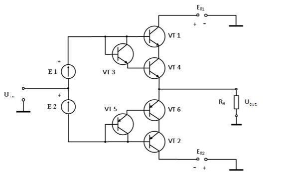
Figure 1. Scheme of the complementary emitter follower to TIVT
To implement the test CEF at TIVT (Figure 1) were used commercially available heterogeneous silicon-based transistors KT-315G (VT1, VT3, VT4) with the structure of n-p-n and KT-361G (VT2, VT5, VT6) the structure of the p-n-p.
The proposed CEF at TIVT works as follows.
Consider the work of TIVT upper arm CEF. Transistor VT1 in the management of the input voltage Ube is in the emitter current control value to set the collector current of transistor IK4 VT4. It works in voltaic injection mode, in which the collector current in the voltage range Ucrit ÷ Uboun not dependent or weakly dependent on the voltage UCB4 (see figure 2, area I characteristics of 1).
VT4 collector potential is always lower than the base potential of transistors VT1 and VT2 on the value of the forward voltage of the emitter-base VT1. Therefore, the intersection of the transistors VT1 and VT4 for any values UCB and UEB, by shifting UEB3 = UCE3 will be located on the horizontal section of the injection voltaic mode (Figure 2), transistors VT3 and VT4 play the role of an ideal generator of stable current feeding emitter transistor VT1.
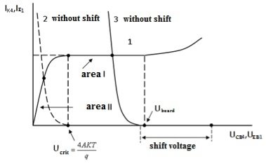
Figure 2. Graph of CVC of transistors TIVT explains the principles of stabilization currents of transistors CEF at TIVT
Results of experimental studies [5] proposed and known CEF has been proven that if you change the values of the external power supply (when Ep1 = EP2) from 5 V to 50 V (for ISK = Ik1 = Ik2 = 1 mA) dissipated at the collector of the upper transistor TIVT power (Pc real = 450 mW) is 3 times greater than the maximum power value in the passport (Pc pass = 150 mW) of the single transistors.
To investigate the amplitude and frequency characteristics of the CEF to TIVT as a power source has been selected dual supply voltage of 20 V and a resistive load Rl=62 Ohm.
Figure 3 shows the combined transfer function study CEF TIVT in the «B«. In study TIVT on CEF, as in known schemes, near zero input voltage current in open TIVT is very small, and internal resistance is big. As a result, increase of the load voltage in this region is smaller than the change in input voltage. This is the cause of the fracture characteristics near zero. Arising from this output voltage distortion is called transient distortion [1]. To eliminate the transient distortion as known, through the transistors pass small quiescent current, i.e., goes to the operating mode «AB».
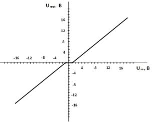
Figure 3. Combined transfer characteristic CEF at TIVT in the mode «B»
In the studied scheme of the CEF to switch to the operating mode «AB» quiescent current of transistors selected as 1mA, which is set with sources of bias E1 and E2.
In figure 4 shown the amplitude response of the CEF to TIVT, when current is 1mA quiescent transistor and fed to the input of the CEF at TIVT harmonic signal with a frequency of 1 kHz. Amplitude characteristic of the investigated schemes is lined enough for practical use, and has the same bending characteristics at high input voltages, as in the scheme known CEF bipolar transistors. This also explains the non-linearity of the current-voltage characteristics of injection voltaic transistors.
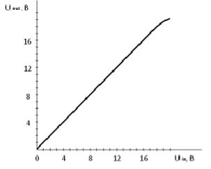
Figure 4. The amplitude characteristic of the CEF on TIVT at EP1=EP2 = 20 V, Ip = 1mA, f0=1kHz, Ui = 6 V and Rl = 620 Ohm
Figure 5 shows the amplitude-frequency characteristic of the investigated schemes as a function of the relative gain from the frequency J = (f), which has the same form as that of the known schemes CEF on single bipolar transistors.
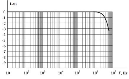
Figure 5. The frequency response of the CEF at TIVT at EP1= EP2 = 20 V, Ip = 1mA, f0=1kHz, Ui = 6 V and Rl = 620 ohm
As we can see from figure 5 the frequency response of the investigated schemes CEF at TIVT is uniform without the «peaks» and «falling» and the upper frequency limit at -3 dB relative gain is equal to 5 MHz.
Conclusion
The results of experimental studies confirm that the use of three structural injection voltaic transistors allows realize highly resistant to the action of destabilizing factors complementary emitter follower and power amplifiers based on them. Three structural injection voltaic transistors have a threefold increase in the safe operating area. Designed complementary emitter follower has a fairly good uniform amplitude-frequency characteristics over a wide frequency range.
References:
- Титце У., Шенк К. Полупроводниковая схемотехника. Справочное руководство. Пер.с нем.-М.: Мир, 1982, стр. 239–242.
- Предварительный патент РУз № IDP 05016. Комплементарный эмиттерный повторитель / Арипов Х. К., Атаханов Ш. Н., Бустанов Х. Х., Касимов С. С., Фазилжанов И. Р. // Бюлл. № 6, 31. 12.2001.
- Фазилжанов И. Р. Исследование комплементарного эмиттерного повторителя с расширенным диапазоном устойчивой работы // Международный Форум. «Новые инфокоммуникационные технологии: достижения, проблемы, перспективы». Том 3. «Техника и технология связи». Тез.докл. международной научно-технической конференции студентов, аспирантов и молодых специалистов стран СНГ.- Новосибирск: СибГУТИ. 2003. С. 33–35.
- Предварительный патент РУз № 5123. Трехструктурный инжекционно-вольтаический транзистор / Арипов Х. К., Бустанов Х. Х., Мавлянов А. Р., Махсудов Д. Т. //. Бюлл. № 2, 30.06.1998.
- Фазилжанов И. Р. Комплементарный эмиттерный повторитель на трехструктурных инжекционно-вольтаических транзисторах // Республиканская научно- техническая конференция аспирантов, магистров и бакалавров «Информационно-коммуникационные технологии». Сб. докладов. — Ташкент, 2008.- C. 196.
